In the fast-paced world of semiconductor manufacturing, where precision and reliability are paramount, choosing a suitable passivation material is critical to ensuring the optimal performance of electronic devices. Among the library of viable materials, glass has gained significant attention for its unique properties and versatility. This article looks at how glass is used for passivation and what properties make it highly suitable for the job.
Understanding Passivation in Semiconductors
Before unpacking the specifics of glass as a material for passivation, it is essential to understand the concept of passivation in semiconductor manufacturing. Passivation involves depositing a protective material onto the surface of metals or metal alloys to enhance their resistance to environmental factors.
The layering material can be organic or inorganic and should exhibit excellent electrical insulation and strong substrate adhesion, as well as block the ingress of chemical species. In the case of semiconductors, passivation is crucial to preventing degradation and ensuring long-term reliability.1,2
Why Use Glass for Passivation?
Glass has emerged as a compelling choice for passivation due to its unique combination of properties. For example, glass can be formulated in numerous ways, with common types including Pb-Si-Al, Zn-B-Si, and Pb-Zn-B. This allows manufacturers to produce glass capable of meeting low and high-voltage electrical specifications; matching the coefficient of thermal expansion of semiconductor materials; and meeting the low temperature processing requirements.3,4
Glass is chemically durable and thus can provide an inert barrier against external elements, such as moisture and contaminants, which might otherwise compromise the semiconductor’s performance. Moreover, the high transparency of some glasses, such as borosilicate glass, makes them ideal for applications with critical optical properties, such as photovoltaics. This transparency enables efficient energy transmission and absorption, contributing to the overall performance of semiconductor devices and solar cells.5,6
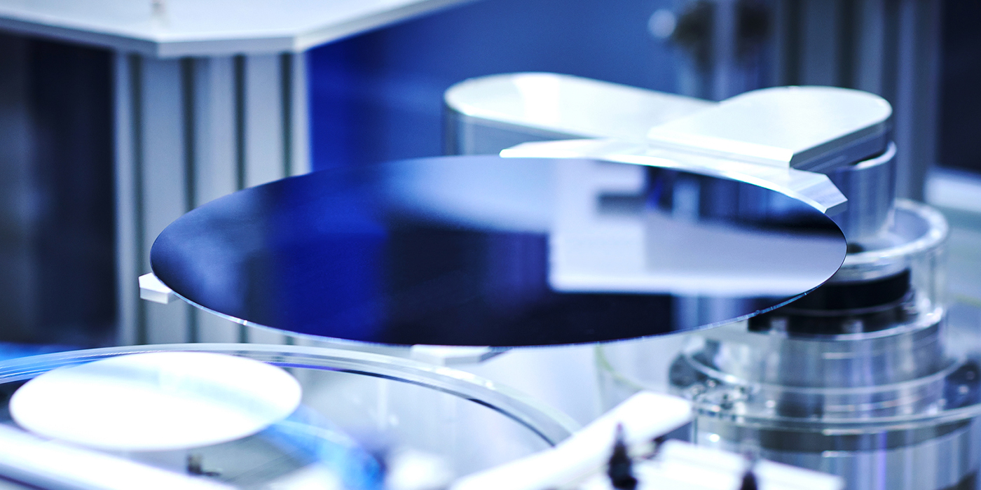
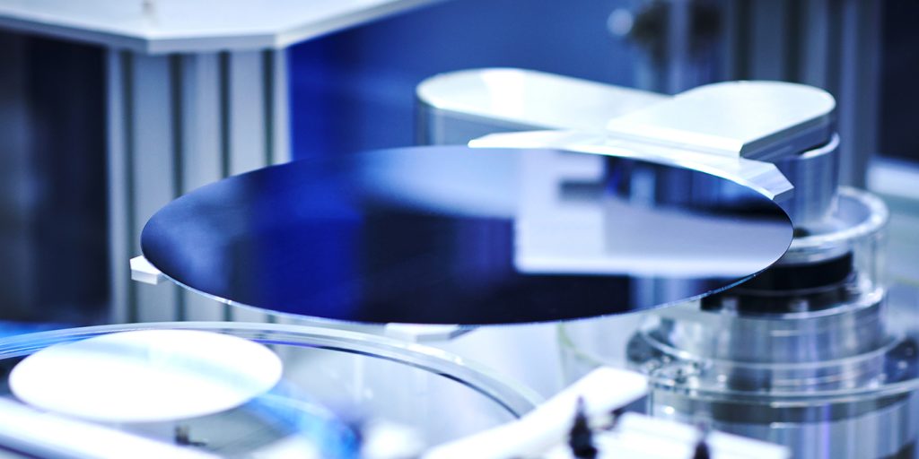
How are Semiconductors Passivated?
Glass can be deposited onto semiconductors in a variety of ways. Choosing methods for passivation depends on factors such as the semiconductor device’s specific requirements, the passivation layer’s desired properties, and the overall manufacturing process. Methods for achieving glass passivation in semiconductor manufacturing include:7
- Chemical vapor deposition (CVD), including plasma-enhanced CVD (PECVD)
- Physical vapor deposition (PVD), including E-beam deposition
- Sputter Coating
- Atomic Layer Deposition (ALD)
In manufacturing, the process of glass passivation is frequently succeeded by chemical procedures, such as the etching of contact windows or the electrolytic deposition of contacts. These procedures may pose a threat to the integrity of the glass.
The chemical resistance of different passivation glasses varies significantly and serves as a crucial factor in determining the suitable glass type and the accompanying etching process.8
Comparing Glass to Other Materials
While various materials can be used for passivation, glass stands out for its exceptional stability over temperature, humidity, and time. Literature searches reveal a lack of head-to-head comparisons with other common passivation materials; however, general comparisons can be drawn.6
Amorphous silicon (a-Si) films utilized in solar cells present numerous advantages. These include a lower deposition temperature, in contrast to the temperatures commonly employed in cell manufacturing. However, it is essential to note that a-Si films exhibit sensitivity to subsequent high-temperature processes, which are frequently necessary in industrial manufacturing technology.9
Similarly, AlOx passivation films can be applied at relatively low temperatures but can be limited by slow deposition speeds when using specific application methods. This can generate problems for high-throughput techniques, such as solar cell production.9
Polyimide, a common passivation material lauded for its strength and thermal stability, is also susceptible to moisture absorption. This can impact the strength and dielectric properties of the protective coating, risking the integrity of the semiconductor.10
Applications of Glass Passivation
Passivation glasses demonstrate outstanding performance in wafer passivation and encapsulation processes, providing advantages to a diverse range of semiconductor devices, including:8
- Thyristors
- Power transistors
- Diodes
- Rectifiers
- Varistors
Glass also has applications in solar cell passivation. In a recent study, researchers developed a method for enhancing borosilicate glass (BSG) passivation using high temperatures before lowering the temperature to accommodate the metallization process. In doing so, they notably improved the solar cell’s efficiency.11
In another study, phosphosilicate glass (PSG) was found to significantly enhance the practical lifetime of minority carriers and improve the overall performance of solar cells, particularly in structures involving nanocrystalline silicon and crystalline silicon.12
Mo-Sci’s Expertise in Glass Thin Films
Fueled by the increasing prevalence of smart devices and advancements in the automotive and aerospace sectors, the semiconductor passivation glass market is anticipated to grow consistently in the next few years.3
Mo-Sci’s expertise lies in leveraging the unique properties of glass to create tailored solutions, ensuring the reliability and performance of many applications, including glass seals and glass coatings. Contact us for more information.
References and Further Reading
- Pehkonen, S.O., et al. (2018). Chapter 2 – Self-Assembly Ultrathin Film Coatings for the Mitigation of Corrosion: General Considerations. Interface Science and Technology. doi.org/10.1016/B978-0-12-813584-6.00002-8
- Lu, Q., et al. (2018). Chapter 5 – Polyimides for Electronic Applications. Advanced Polyimide Materials. doi.org/10.1016/B978-0-12-812640-0.00005-6
- Reliable Business Insights. [Online] Semiconductor Passivation Glass Market – Global Outlook and Forecast 2023-2028. Available at: https://www.reliablebusinessinsights.com/purchase/1365249?utm_campaign=2&utm_medium=cp_9&utm_source=Linkedin&utm_content=ia&utm_term=semiconductor-passivation-glass&utm_id=free (Accessed on 05 January 2024).
- Schott. [Online] Passivation Glass. Available at: https://www.schott.com/en-hr/products/passivation-glass-p1000287/technical-details (Accessed on 05 January 2024).
- Zhong, C., et al. (2022). Properties and mechanism of amorphous lead aluminosilicate passivation layers used in semiconductor devices through molecular dynamic simulation. Ceramics International. doi.org/10.1016/j.ceramint.2022.07.191
- Hansen, U., et al. (2009). Robust and Hermetic Borosilicate Glass Coatings by E-Beam Evaporation. Procedia Chemistry. doi.org/10.1016/j.proche.2009.07.019
- Korvus Technology. [Online] The Revolution of PVD Systems in Thin Film Semiconductor Production. Available at: https://korvustech.com/thin-film-semiconductor/ (Accessed on 05 January 2024).
- Schott. Technical Glasses: Physical and Technical Properties. Available at: https://www.schott.com/-/media/project/onex/shared/downloads/melting-and-hot-forming/390768-row-schott-technical-glasses-view-2020-04-14.pdf?rev=-1
- Bonilla, R.S., et al. (2017). Dielectric surface passivation for silicon solar cells: A review. Physica Status Solidi. doi.org/10.1002/pssa.201700293
- Babu, S.V., et al. (1993). Reliability of Multilayer Copper/Polyimide. Defense Technical Information Centre. Available at: https://apps.dtic.mil/sti/citations/ADA276228
- Liao, B., et al. (2021). Unlocking the potential of boronsilicate glass passivation for industrial tunnel oxide passivated contact solar cells. Progress in Photovoltaics. doi.org/10.1002/pip.3519
- Imamura, K., et al. (2018). Effective passivation for nanocrystalline Si layer/crystalline Si solar cells by use of phosphosilicate glass. Solar Energy. doi.org/10.1016/j.solener.2018.04.063